- Ultra Wide Bandgap Semiconductors (Ga2O3): Synthesis, Characterization and Device Applications
- MOCVD of II-IV-Nitride and II-IV-Nitride/III-Nitride Heterostructures for Next Generation of Optoelectronics
- Synthesis of Low-Dimensional Wide Bandgap Nanostructures & Device Applications
- Light-Matter Interactions at Interface of Optoelectronic Devices
- QW Engineering for Enhancing III-nitride LED Quantum Efficiency
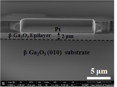
Ultra Wide Bandgap Semiconductors (Ga2O3): Synthesis, Characterization and Device Applications
Ultra wide band gap Ga2O3 (Eg ∼4.5- 4.9 eV, direct) is a material with excellent chemical and thermal stability up to 1400 oC. The monoclinic of β-phase Ga2O3 represents the thermally stable crystal among the known five phases. The breakdown field of β-Ga2O3 is estimated to be 6-8 MV/cm, which is about three times larger than those of 4H-SiC and GaN. We achieved the synthesis of high quality single crystalline β-Ga2O3 thin films with growth rate (> 5 µm/hr) with room temperature electron mobility of >100 cm2/Vs via low pressure chemical vapor deposition.

MOCVD of II-IV-Nitride and II-IV-Nitride/III-Nitride Heterostructures for Next Generation of Optoelectronics (Collaborating with Profs. Kathleen Kash and Walter Lambrecht)
As a close family to III-nitride, the new cluster II-IV-nitride (e.g. ZnGeN2, ZnSnN2) semiconductors have similar crystal structure and band gap energies to that of III-nitride. Nevertheless, there are compelling reasons for the interest in the II-IV-nitrides. For example, the spontaneous polarization coefficients along the c axis of Zn-IV-N2 are predicted to be an order of magnitude smaller than for the III-nitrides. The doping properties of II-IV-nitride is speculated to be very different from III-nitride. ZnGeP2 and ZnGeN2 may be intrinsically p-type due to Zn vacancies, which has continued to prove difficult to achieve for the large bandgap III-nitrides. Similarly, the etching properties of II-IV-nitride are predicted to be very different from III-nitride, which could only rely on dry etching. In addition, their close lattice match over a wide range of the alloys makes them a good choice for incorporation into III-V/III-nitride heterostructures.


Synthesis of Low-Dimensional Wide Bandgap Nanostructures & Device Applications
III-nitride nanowires with 1D structure are explored with unique properties of 1) large surface-to-volume ratio; 2) better stoichiometrically controlled and greater level of crystallinity than 2D thin film; 3) better control of defects on various substrates than 2D thin film; and 4) low cost and high compatibility with microelectronics for integration to system level. Fundamental growth mechanisms are explored with the goal to realize controllable synthesis of III-nitride NWs for optoelectronic and electronic device applications.

![]()


Light-Matter Interactions at Interface of Optoelectronic Devices
In light-emitting diodes (LEDs), a large amount of light generated in the semiconductor active region is trapped within the high-index semiconductor material, leading to low light extraction efficiency, which limits the total device efficiency significantly.
III-nitride microspheres and micro-domes were implemented into both visible InGaN quantum wells (QWs) LEDs and ultraviolet (UV) AlGaN QWs LEDs for enhancing light extraction efficiency. Numerical calculation based on three-dimensional finite difference time domain (3D-FDTD) method was used to study and optimize the micro-dome surface feature for both thin-film-flip-chip InGaN LEDs and deep-UV AlGaN LEDs, which shows great promise to enhance light extraction efficiency for these devices. Experimental exploration to form desired GaN micro-domes utilized self-assembled dip-coating deposition of SiO2 microspheres as masks and plasma dry etching to simultaneously etch both mask material and GaN substrate, which demonstrated the feasibility to implement the III-nitride micro-domes into III-nitride based optoelectronic devices.


QW Engineering for Enhancing III-nitride LED Quantum Efficiency
The band bending for both conduction band and valence band due to the existence of polarizations leads to significantly reduced electron-hole wavefunction overlap and spontaneous emission radiative recombination rate in InGaN QWs. The concept of large overlap QW design is implemented to enhance the internal quantum efficiency in InGaN QW based LEDs. Two approaches are used to address this issue: 1. use of inter-diffused InGaN QWs; and 2. use of asymmetric InGaN-delta-InN QWs.
1. Inter-diffused InGaN QWs
The interdiffusion of indium and gallium between InGaN QWs and GaN barriers significantly modifies the energy band lineups for InGaN QWs, which leads to the shift of both electron and hole wavefunctions, resulting in enhancement of the electron-hole wavefunction overlap. With the error-function like interface band lineups, the interdiffused InGaN QWs show enhanced electron-hole wavefunction overlap as compare to that of the conventional InGaN QWs emitting at similar wavelength. The interdiffusion, which is achievable by rapid thermal annealing, provides a cost-effective approach to engineer the QW band structures for enhancing the QW performance, which has great potential to achieve InGaN QW based LEDs with improved radiative recombination rate and radiative efficiency emitting applicable for solid state lighting.


2. Asymmetric InGaN-delta-InN QWs
By inserting an ultrathin narrow band gap delta-InN layer in the InGaN QW, the InGaN-delta-InN QW forms a local potential minima in the QW, which leads to strong confinement of both electrons and holes in the QW. The effects of delta-InN layer positions and thicknesses on the spontaneous emission radiative recombination properties in InGaN-delta-InN QW have been comprehensively analyzed. Both inter-band transition wavelength and spontaneous emission intensity significantly depend on the delta-InN layer position and thickness in the InGaN-delta-InN QW. The design of the InGaN-delta-InN QW has great potential to realize high performance InGaN QW based LEDs emitting in green, yellow, red and beyond.


